
 Technology peripherals
It Industry
SK hynix's innovative semiconductor CMP polishing pad technology enables sustainable use
Technology peripherals
It Industry
SK hynix's innovative semiconductor CMP polishing pad technology enables sustainable use
SK hynix's innovative semiconductor CMP polishing pad technology enables sustainable use
Dec 28, 2023 pm 11:04 PM
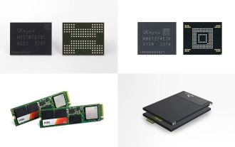
According to news from this website on December 27, according to Korean media ETNews, SK Hynix has recently developed reusable CMP polishing pad technology, which can not only reduce costs, but also enhance ESG (environmental) , society, governance) management.
SK Hynix stated that they will first deploy reusable CMP polishing pads in low-risk processes and gradually expand their application scope
Note on this site: CMP technology is to enable polished It is a process in which the surface of the material reaches the required flatness under the combined action of chemistry and machinery. The chemical components in the polishing fluid react chemically with the material surface to form a softened layer that is easy to polish. The polishing pad and abrasive particles in the polishing fluid physically and mechanically polish the material surface to remove the softened layer.
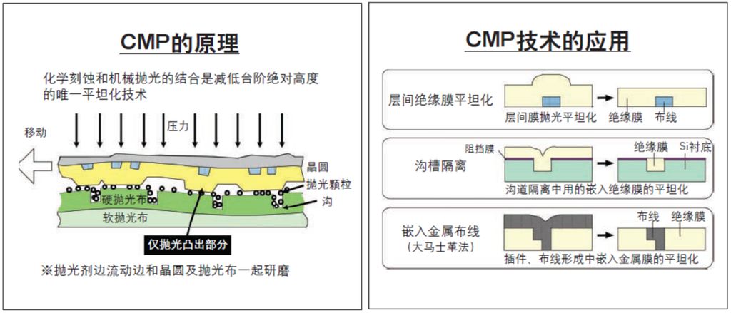
In the CMP process, the main functions of the polishing pad are:
In order to achieve uniform distribution of the polishing fluid to the entire processing area and provide new supplementary polishing fluid for circulation, the following operations need to be performed:
Clear due to the polishing process The resulting residues on the workpiece surface, such as polishing chips, chips, etc.
Need to eliminate the required mechanical load when transferring the material;
It is very important to maintain the mechanical and chemical environment required for the polishing process. In addition to the mechanical properties of the polishing pad, the structural characteristics of the surface also have an impact on polishing efficiency and flatness. For example, the shape of micropores, porosity, and groove shape will affect the flow and distribution of the polishing fluid
SK Hynix uses the CMP polishing pad dial texture reconstruction method to ensure Polishing pads can be reused
About 70% of CMP polishing pads in South Korea use foreign products and are highly dependent on foreign countries. However, by breaking through this technology, the further independent development of the Korean semiconductor industry can be promoted
The above is the detailed content of SK hynix's innovative semiconductor CMP polishing pad technology enables sustainable use. For more information, please follow other related articles on the PHP Chinese website!

Hot AI Tools

Undress AI Tool
Undress images for free

Undresser.AI Undress
AI-powered app for creating realistic nude photos

AI Clothes Remover
Online AI tool for removing clothes from photos.

Clothoff.io
AI clothes remover

Video Face Swap
Swap faces in any video effortlessly with our completely free AI face swap tool!

Hot Article
Hot Tools

Notepad++7.3.1
Easy-to-use and free code editor

SublimeText3 Chinese version
Chinese version, very easy to use

Zend Studio 13.0.1
Powerful PHP integrated development environment

Dreamweaver CS6
Visual web development tools

SublimeText3 Mac version
God-level code editing software (SublimeText3)
Hot Topics


 Sources say SK Hynix's five-layer stacked 3D DRAM memory yield has reached 56.1%
Jun 24, 2024 pm 01:52 PM
Sources say SK Hynix's five-layer stacked 3D DRAM memory yield has reached 56.1%
Jun 24, 2024 pm 01:52 PM
According to news from this website on June 24, Korean media BusinessKorea reported that industry insiders revealed that SK Hynix published the latest research paper on 3D DRAM technology at the VLSI 2024 Summit held in Hawaii, USA from June 16 to 20. In this paper, SK Hynix reports that its five-layer stacked 3D DRAM memory yield has reached 56.1%, and the 3D DRAM in the experiment exhibits similar characteristics to current 2D DRAM. According to reports, unlike traditional DRAM, which arranges memory cells horizontally, 3D DRAM stacks cells vertically to achieve higher density in the same space. However, SK hynix
 TrendForce: Nvidia's Blackwell platform products drive TSMC's CoWoS production capacity to increase by 150% this year
Apr 17, 2024 pm 08:00 PM
TrendForce: Nvidia's Blackwell platform products drive TSMC's CoWoS production capacity to increase by 150% this year
Apr 17, 2024 pm 08:00 PM
According to news from this site on April 17, TrendForce recently released a report, believing that demand for Nvidia's new Blackwell platform products is bullish, and is expected to drive TSMC's total CoWoS packaging production capacity to increase by more than 150% in 2024. NVIDIA Blackwell's new platform products include B-series GPUs and GB200 accelerator cards integrating NVIDIA's own GraceArm CPU. TrendForce confirms that the supply chain is currently very optimistic about GB200. It is estimated that shipments in 2025 are expected to exceed one million units, accounting for 40-50% of Nvidia's high-end GPUs. Nvidia plans to deliver products such as GB200 and B100 in the second half of the year, but upstream wafer packaging must further adopt more complex products.
 Innolux plans to mass-produce fan-out panel-level semiconductor packaging technology by the end of the year
Aug 07, 2024 pm 06:18 PM
Innolux plans to mass-produce fan-out panel-level semiconductor packaging technology by the end of the year
Aug 07, 2024 pm 06:18 PM
According to news from this site on August 6, Yang Zhuxiang, general manager of Innolux Corporation, said yesterday (August 5) that the company is actively deploying and promoting semiconductor fan-out panel-level packaging (FOPLP) and is expected to mass-produce ChipFirst before the end of this year. The contribution of process technology to revenue will be apparent in the first quarter of next year. Fenye Innolux stated that it is expected to mass-produce the redistribution layer (RDLFirst) process technology for mid-to-high-end products in the next 1-2 years, and will work with partners to develop the most technically difficult glass drilling (TGV) process, which will take another 2-3 years. It can be put into mass production within a year. Yang Zhuxiang said that Innolux’s FOPLP technology is “ready for mass production” and will enter the market with low-end and mid-range products.
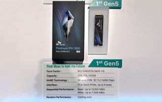 SK Hynix demonstrates Platinum P51 SSD: sequential read peak 13500 MB/s
Mar 20, 2024 pm 02:36 PM
SK Hynix demonstrates Platinum P51 SSD: sequential read peak 13500 MB/s
Mar 20, 2024 pm 02:36 PM
According to news from this website on March 20, SK Hynix recently attended the NVIDIA GTC2024 conference and demonstrated the first Gen5NVMe solid-state drive series for the consumer market-Platinum P51M.22280NVMeSSD. PlatinumP51 is similar to GoldP31 and PlatinumP41. It uses a self-designed SSD master control, but the main highlight is the use of PCIeGen5 and 238-layer TLCNAND flash memory. Note from this site: Hynix acquired SSD master control manufacturer LAMD in 2012, giving it the ability to design its own master control. SK Hynix said at the booth that Platinum P51 will be launched in 500GB, 1TB and 2
 SK Hynix will display new AI-related products on August 6: 12-layer HBM3E, 321-high NAND, etc.
Aug 01, 2024 pm 09:40 PM
SK Hynix will display new AI-related products on August 6: 12-layer HBM3E, 321-high NAND, etc.
Aug 01, 2024 pm 09:40 PM
According to news from this site on August 1, SK Hynix released a blog post today (August 1), announcing that it will attend the Global Semiconductor Memory Summit FMS2024 to be held in Santa Clara, California, USA from August 6 to 8, showcasing many new technologies. generation product. Introduction to the Future Memory and Storage Summit (FutureMemoryandStorage), formerly the Flash Memory Summit (FlashMemorySummit) mainly for NAND suppliers, in the context of increasing attention to artificial intelligence technology, this year was renamed the Future Memory and Storage Summit (FutureMemoryandStorage) to invite DRAM and storage vendors and many more players. New product SK hynix launched last year
 SK hynix's innovative semiconductor CMP polishing pad technology enables sustainable use
Dec 28, 2023 pm 11:04 PM
SK hynix's innovative semiconductor CMP polishing pad technology enables sustainable use
Dec 28, 2023 pm 11:04 PM
According to news from this website on December 27, according to Korean media ETNews, SK Hynix has recently developed reusable CMP polishing pad technology, which can not only reduce costs, but also enhance ESG (environmental, social, governance) management. SK Hynix said that they will first deploy reusable CMP polishing pads in low-risk processes and gradually expand their application scope. Note: CMP technology is to make the surface of the material to be polished under the combined action of chemicals and mechanics. A process to achieve the required flatness. The chemical components in the polishing fluid react chemically with the material surface to form a softened layer that is easy to polish. The polishing pad and abrasive particles in the polishing fluid physically and mechanically polish the material surface to remove the softened layer. Source: Dinglong shares in CM
 Sony Group: Its semiconductor factories concealed emissions of harmful substances
Jul 12, 2024 pm 02:09 PM
Sony Group: Its semiconductor factories concealed emissions of harmful substances
Jul 12, 2024 pm 02:09 PM
According to reports from this website on July 8, based on reports from Nikkei and Japan's "Jiji News Agency", on the 8th (today) local time, Sony Semiconductor Manufacturing Company, a semiconductor manufacturer under the Sony Group, announced that the company had discharged harmful chemicals outside the factory. , and no notification was made. The company said this was due to an input error and an imperfect confirmation system. In fiscal years 2021 and 2022, the camera image sensor factory located in Kikuyo Town, Kumamoto Prefecture, incorrectly reported its emissions of chemical substances as 0. The actual situation was that there were emissions of "waste without harmless treatment." The plant emits hydrogen fluoride, which is commonly used in semiconductor processing and cleaning. Note from this site: Hydrogen fluoride is harmful to the human body and can cause respiratory diseases and even life-threatening effects when inhaled. sony half
 It is reported that Pioneer International Semiconductor acquires AUO's Singapore factory to build an advanced 12-inch automotive chip wafer fab
Oct 31, 2023 pm 12:37 PM
It is reported that Pioneer International Semiconductor acquires AUO's Singapore factory to build an advanced 12-inch automotive chip wafer fab
Oct 31, 2023 pm 12:37 PM
According to news from this site on October 31, the Economic Daily learned from industry insiders that Pioneer International Semiconductor/World Advanced (VIS) is currently negotiating with AUO's Singapore factory to acquire the land and equipment held by the latter and use it to Construction of the first 12-inch wafer fab. Source: AUO’s official website Pioneer International Semiconductor plans to invest US$2 billion (approximately RMB 14.64 billion) to produce chips, mainly for the automotive field. According to reports, Pioneer International Semiconductor will hold a relevant meeting on November 7. AUO plans to hold a relevant meeting on October 31. The two companies have not yet issued official comments on the relevant rumors. Reports indicate that AUO plans to gradually withdraw its development focus in Singapore from manufacturing to establishing a regional service center. This Singapore factory was established in 201
