


JAVA programs run on virtual machines and require memory space when running. When a virtual machine executes a JAVA program, the memory it manages is divided into different data areas for easy management. The virtual machine management memory data area is divided into the following figure:

Java learning video recommendation: java online tutorial
1. Program Counter Register
Line number indicator, branch, loop, jump, exception handling, thread recovery (CPU switching) of bytecode instructions, each thread requires an independent The counter and thread private memory do not affect each other, and no memory overflow exception will occur in this area.
2. Virtual Machine Stack (VM Stack)
The virtual machine stack (VM Stack) is private to the thread. The declaration period is the same as the thread. The virtual machine stack is Java Memory model of method execution. When each method is executed, a stack frame is created, which is the basic data structure during method execution.
The stack frame is used to store: local variable table, operand stack, dynamic link, method exit, etc. The execution of each method corresponds to the process of the virtual machine stack frame from the stack to the stack. It is a data structure, a local variable table in the virtual machine, corresponding to the program data model above the physical layer.
The local variable table is a program running data model that stores various data types known during compilation, such as:
Boolean, byte, char, short, int, float, long, Double, object reference type (object memory address variable, pointer or handle). When the program is running, the stack frame space size is allocated according to the local variable table. During operation, the size is unchanged. Exception type: stackOverFlowError. The thread request stack depth is greater than the virtual machine allowed depth. OutOfMemory The memory space is exhausted and cannot be expanded.
3. Native Method Stack
Similar to the virtual machine stack, the virtual machine stack serves Java programs, and the local method stack supports the running of the virtual machine The specific implementation of the service is determined by the virtual machine manufacturer and will also throw stackOverFlowError and OutOfMemory exceptions.
4. Heap
The Heap is the largest part of the memory managed by the virtual machine. It is shared by all threads and is used to store object instances (objects). , array), physically discontinuous memory space. Since the GC collector collects in generations, it is divided into: new generation Eden, From SurVivor space, To SurVivor space, allot buffer (allocation space), which may be divided into multiple Thread-private buffer, old generation.
5. Method Area
The method area (Method Area), like the heap area, is a thread-shared memory area and is used to store data loaded by the virtual machine. Class information, constants, static variables, code compiled by the just-in-time compiler (dynamically loaded OSGI) and other data. Theoretically, it is part of the Java virtual machine. To distinguish it, it is called Non-Heap.
You can choose not to perform garbage collection in this area. The purpose of recycling in this area is mainly to recycle the constant pool and uninstall classes. When the memory area is insufficient, an OutOfMemory exception will be thrown.
Runtime constant pool: part of the method area, Class version, fields, interfaces, methods, etc., as well as various literals and symbol references generated during compilation, which are stored in this area after the compiled class is loaded. OutOfMemory exception will be thrown.
6. Direct Memory
Direct Memory does not belong to the virtual memory area. It is an IO method based on channels and buffers. You can use native functions to directly allocate off-heap memory, store the referenced external memory address in the heap, and complete the operation of directly referenced memory through references. The NIO provided after 1.4 significantly improves efficiency and avoids the back-and-forth copy operation between heap memory and Native memory. , not controlled by the virtual machine memory, will throw an OUTOfMemory exception.
Recommended related article tutorials: Getting started with java development
The above is the detailed content of An in-depth introduction to the JVM memory data area. For more information, please follow other related articles on the PHP Chinese website!

Hot AI Tools

Undress AI Tool
Undress images for free

Undresser.AI Undress
AI-powered app for creating realistic nude photos

AI Clothes Remover
Online AI tool for removing clothes from photos.

Clothoff.io
AI clothes remover

Video Face Swap
Swap faces in any video effortlessly with our completely free AI face swap tool!

Hot Article
Hot Tools

Notepad++7.3.1
Easy-to-use and free code editor

SublimeText3 Chinese version
Chinese version, very easy to use

Zend Studio 13.0.1
Powerful PHP integrated development environment

Dreamweaver CS6
Visual web development tools

SublimeText3 Mac version
God-level code editing software (SublimeText3)


 Large memory optimization, what should I do if the computer upgrades to 16g/32g memory speed and there is no change?
Jun 18, 2024 pm 06:51 PM
Large memory optimization, what should I do if the computer upgrades to 16g/32g memory speed and there is no change?
Jun 18, 2024 pm 06:51 PM
For mechanical hard drives or SATA solid-state drives, you will feel the increase in software running speed. If it is an NVME hard drive, you may not feel it. 1. Import the registry into the desktop and create a new text document, copy and paste the following content, save it as 1.reg, then right-click to merge and restart the computer. WindowsRegistryEditorVersion5.00[HKEY_LOCAL_MACHINE\SYSTEM\CurrentControlSet\Control\SessionManager\MemoryManagement]"DisablePagingExecutive"=d
 Sources say Samsung Electronics and SK Hynix will commercialize stacked mobile memory after 2026
Sep 03, 2024 pm 02:15 PM
Sources say Samsung Electronics and SK Hynix will commercialize stacked mobile memory after 2026
Sep 03, 2024 pm 02:15 PM
According to news from this website on September 3, Korean media etnews reported yesterday (local time) that Samsung Electronics and SK Hynix’s “HBM-like” stacked structure mobile memory products will be commercialized after 2026. Sources said that the two Korean memory giants regard stacked mobile memory as an important source of future revenue and plan to expand "HBM-like memory" to smartphones, tablets and laptops to provide power for end-side AI. According to previous reports on this site, Samsung Electronics’ product is called LPWide I/O memory, and SK Hynix calls this technology VFO. The two companies have used roughly the same technical route, which is to combine fan-out packaging and vertical channels. Samsung Electronics’ LPWide I/O memory has a bit width of 512
 Samsung announced the completion of 16-layer hybrid bonding stacking process technology verification, which is expected to be widely used in HBM4 memory
Apr 07, 2024 pm 09:19 PM
Samsung announced the completion of 16-layer hybrid bonding stacking process technology verification, which is expected to be widely used in HBM4 memory
Apr 07, 2024 pm 09:19 PM
According to the report, Samsung Electronics executive Dae Woo Kim said that at the 2024 Korean Microelectronics and Packaging Society Annual Meeting, Samsung Electronics will complete the verification of the 16-layer hybrid bonding HBM memory technology. It is reported that this technology has passed technical verification. The report also stated that this technical verification will lay the foundation for the development of the memory market in the next few years. DaeWooKim said that Samsung Electronics has successfully manufactured a 16-layer stacked HBM3 memory based on hybrid bonding technology. The memory sample works normally. In the future, the 16-layer stacked hybrid bonding technology will be used for mass production of HBM4 memory. ▲Image source TheElec, same as below. Compared with the existing bonding process, hybrid bonding does not need to add bumps between DRAM memory layers, but directly connects the upper and lower layers copper to copper.
 Kingbang launches new DDR5 8600 memory, offering CAMM2, LPCAMM2 and regular models to choose from
Jun 08, 2024 pm 01:35 PM
Kingbang launches new DDR5 8600 memory, offering CAMM2, LPCAMM2 and regular models to choose from
Jun 08, 2024 pm 01:35 PM
According to news from this site on June 7, GEIL launched its latest DDR5 solution at the 2024 Taipei International Computer Show, and provided SO-DIMM, CUDIMM, CSODIMM, CAMM2 and LPCAMM2 versions to choose from. ▲Picture source: Wccftech As shown in the picture, the CAMM2/LPCAMM2 memory exhibited by Jinbang adopts a very compact design, can provide a maximum capacity of 128GB, and a speed of up to 8533MT/s. Some of these products can even be stable on the AMDAM5 platform Overclocked to 9000MT/s without any auxiliary cooling. According to reports, Jinbang’s 2024 Polaris RGBDDR5 series memory can provide up to 8400
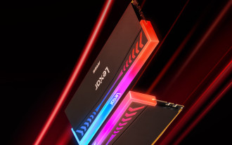 Lexar launches Ares Wings of War DDR5 7600 16GB x2 memory kit: Hynix A-die particles, 1,299 yuan
May 07, 2024 am 08:13 AM
Lexar launches Ares Wings of War DDR5 7600 16GB x2 memory kit: Hynix A-die particles, 1,299 yuan
May 07, 2024 am 08:13 AM
According to news from this website on May 6, Lexar launched the Ares Wings of War series DDR57600CL36 overclocking memory. The 16GBx2 set will be available for pre-sale at 0:00 on May 7 with a deposit of 50 yuan, and the price is 1,299 yuan. Lexar Wings of War memory uses Hynix A-die memory chips, supports Intel XMP3.0, and provides the following two overclocking presets: 7600MT/s: CL36-46-46-961.4V8000MT/s: CL38-48-49 -1001.45V In terms of heat dissipation, this memory set is equipped with a 1.8mm thick all-aluminum heat dissipation vest and is equipped with PMIC's exclusive thermal conductive silicone grease pad. The memory uses 8 high-brightness LED beads and supports 13 RGB lighting modes.
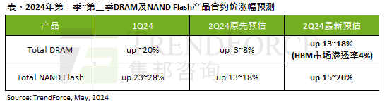 The impact of the AI ??wave is obvious. TrendForce has revised up its forecast for DRAM memory and NAND flash memory contract price increases this quarter.
May 07, 2024 pm 09:58 PM
The impact of the AI ??wave is obvious. TrendForce has revised up its forecast for DRAM memory and NAND flash memory contract price increases this quarter.
May 07, 2024 pm 09:58 PM
According to a TrendForce survey report, the AI ??wave has a significant impact on the DRAM memory and NAND flash memory markets. In this site’s news on May 7, TrendForce said in its latest research report today that the agency has increased the contract price increases for two types of storage products this quarter. Specifically, TrendForce originally estimated that the DRAM memory contract price in the second quarter of 2024 will increase by 3~8%, and now estimates it at 13~18%; in terms of NAND flash memory, the original estimate will increase by 13~18%, and the new estimate is 15%. ~20%, only eMMC/UFS has a lower increase of 10%. ▲Image source TrendForce TrendForce stated that the agency originally expected to continue to
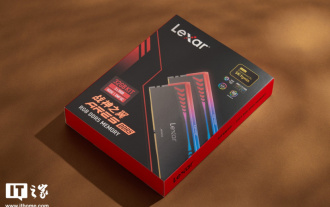 Lexar God of War Wings ARES RGB DDR5 8000 Memory Picture Gallery: Colorful White Wings supports RGB
Jun 25, 2024 pm 01:51 PM
Lexar God of War Wings ARES RGB DDR5 8000 Memory Picture Gallery: Colorful White Wings supports RGB
Jun 25, 2024 pm 01:51 PM
When the prices of ultra-high-frequency flagship memories such as 7600MT/s and 8000MT/s are generally high, Lexar has taken action. They have launched a new memory series called Ares Wings ARES RGB DDR5, with 7600 C36 and 8000 C38 is available in two specifications. The 16GB*2 sets are priced at 1,299 yuan and 1,499 yuan respectively, which is very cost-effective. This site has obtained the 8000 C38 version of Wings of War, and will bring you its unboxing pictures. The packaging of Lexar Wings ARES RGB DDR5 memory is well designed, using eye-catching black and red color schemes with colorful printing. There is an exclusive &quo in the upper left corner of the packaging.
 DDR5 MRDIMM and LPDDR6 CAMM memory specifications are ready for launch, JEDEC releases key technical details
Jul 23, 2024 pm 02:25 PM
DDR5 MRDIMM and LPDDR6 CAMM memory specifications are ready for launch, JEDEC releases key technical details
Jul 23, 2024 pm 02:25 PM
According to news from this website on July 23, the JEDEC Solid State Technology Association, the microelectronics standard setter, announced on the 22nd local time that the DDR5MRDIMM and LPDDR6CAMM memory technical specifications will be officially launched soon, and introduced the key details of these two memories. The "MR" in DDR5MRDIMM stands for MultiplexedRank, which means that the memory supports two or more Ranks and can combine and transmit multiple data signals on a single channel without additional physical The connection can effectively increase the bandwidth. JEDEC has planned multiple generations of DDR5MRDIMM memory, with the goal of eventually increasing its bandwidth to 12.8Gbps, compared with the current 6.4Gbps of DDR5RDIMM memory.
